Introduction
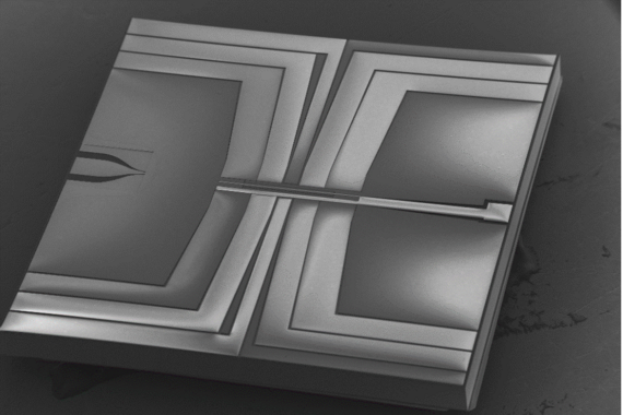
We fabricate surface-electrode traps at PTB's clean room facility and in the LNQE clean room. Our trap fabrication involves metal deposition, structuring using photolithography and different wet and dry etching techniques. For diagnostics, we employ scanning electron microscopy (SEM), optical microscopy and contact profilometry.
Different substrates, including aluminum nitride and high resistivity silicon, can be used. Our surface-electrode traps use electroplated gold as the electrode material. We have fabricated both single and multilayer traps.


Single-layer surface electrode ion traps
We use conventional microfabrication techniques to fabricate single-layer surface-electrode ion traps [3]. Initially, a dielectric substrate, typically Aluminium Nitride (AlN), is coated with a bilayer thin film composed of titanium and gold. The first acts as a good adhesion layer to hold the trap structures. The second one plays an important role as a starting conductive layer. Followed by a photolithography step, in which parts of a previously UV-exposed resist are exposed on the conductive layer, the substrate is placed in an electrolyte solution to grow gold electrodes by electroplating.
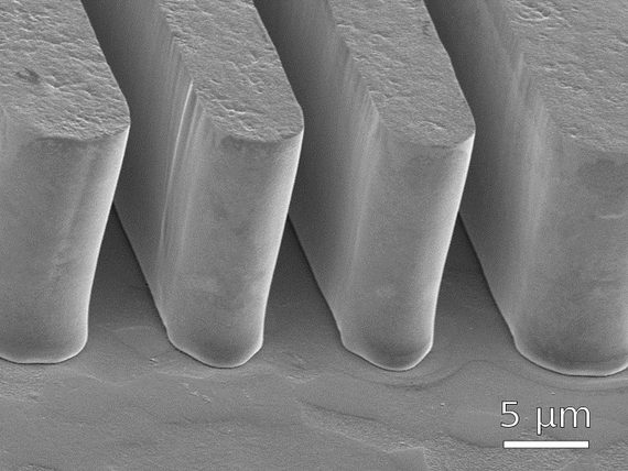
This method allows the possibility of building large (height-to-width) aspect ratio structures. As shown in the picture on the left, trap features as thick as 15 µm and gaps of about 3 µm can be fabricated.
References
- [1] D. Kielpinski, C. Monroe, and D. J. Wineland, Nature 417, 709–711 (2002)
- [2] J. M. Amini et al., New J. Phys. 12, 033031 (2010)
- [3] M. Wahnschaffe et al., Appl. Phys. Lett. 110, 034103 (2017)
- [4] S. Seidelin et al., Phys. Rev. Lett. 96, 253003, (2006)
- [5] A. Bautista-Salvador et al., arXiv:1812.01829 (2018)


